Pin
Name
Description
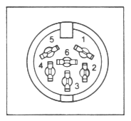
1
SRQ
Serial Service Request
2
GND
Ground
3
ATN
Serial Attention
4
CLK
Serial Clock
5
DATA
Serial Data
6
RESET
Serial Reset
The Theory
Serial Bus Lines
Pin |
Name |
Description |
|
1 |
SRQ |
Serial Service Request |
|
2 |
GND |
Ground |
|
3 |
ATN |
Serial Attention |
|
4 |
CLK |
Serial Clock |
|
5 |
DATA |
Serial Data |
|
6 |
RESET |
Serial Reset |
Pin 1 is called Serial Service Request and is not used
Pin 2 is connected to the interfaces ground
Pin 3, 4, 5 and 6 are the main pins we are working with. They are responsible
for the reset and the data transmission.
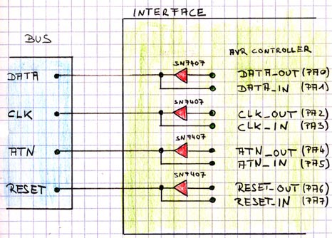
The serial interface must be able to set and read these lines, so we have to connect them to a port of our AVR controller. This is not done directly, because the modern technology of the AVR controller seems to be incompatible to the old technology of our 1541 drive or the Commodore 64. So it is done in the same way as in the Commodore 64 and the 1541. We connect the port lines to some SN7407 buffers. The following picture shows the complete line setup and the connection to PORT A of the Atmel controller.
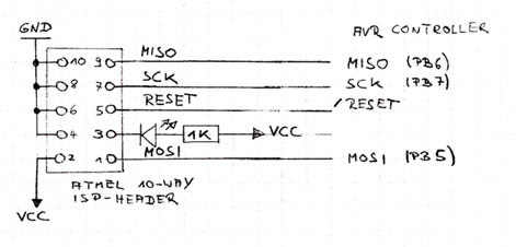
The AVR controller has to be programmed. We have to write the firmware to the controllers flash-memory. This can be done with an AVR programmer. The STK500 starterkit from Atmel has such a programmer on board, but you can also build your own device or buy a programmer. You can download AVR Studio from the Atmel website. With AVR Studio you can compile your code and program all AVR devices, including our ATMega8535. To be able to reprogram the controller once it is soldered into our PCB, there is a 10 pin ISP Header on the interface (for In System Programming). This ISP Header has to be connected to the STK500 or to any other AVR-programmer. When the interface was connected to the programmer, it can be programmed with AVR Studio 4. Here is a picture of the ISP Header on the 1541 interface:
The data transfer between interface and PC is very easy. The serial port from the PC side is connected to a MAX232CPE chip, which is translating the voltages from and to TTL level (5V). The MAX232 is connected to the controllers UART. The following picture shows, how the lines are connected:
The two possible voltages on each line are 0V or 5V. In the following sections, if a line is SET, then its voltage is set to 5V. If a line is CLEARED, its voltage is set to 0V. If a line is “released“, then its voltage is set to 5V. If a line is “pulled down”, then its voltage is set to 0V. “Released” is 5V, because the Commodore 64 serial bus is “active low”. This means, if a line has a voltage of 5V some device on the bus can pull it down to 0V. But if one device is pulling it down to 0V no other device can set it back to 5V. Only the device that pulled the line down can release the line (set it back to 5V). HIGH means 5V and LOW means 0V.
There are 4 basic commands, that can be sent to the floppy. LISTEN,TALK,UNLISTEN and UNTALK.
A command is sent to the floppy by transfering a command byte. One difference from sending a “normal” byte is, that the ATN-Line is LOW while the byte is sent. When sending a normal byte, the ATN-Line is HIGH. In addition we have to do the following, before sending the byte: Clear the Clock-Line, set the Data-Line and wait for about 754 cycles.
Command |
Byte to send while ATN is LOW |
LISTEN |
$20 + DEVICE-NUMBER |
TALK |
$40 + DEVICE-NUMBER |
UNLISTEN |
$3F |
UNTALK |
$5F |
ED09 09 40 ORA #$40 ; TALK (IEC) A=Devicenumber + $20 => LISTEN Command Byte
ED0B .BY
$2C ; skip next 2 bytes
(skip the listen stuff
)
ED17 66
A3 ROR $A3 ; dont care
ED1C 46
94 LSR $94 ;
dont care
ED20 68
PLA ; get commandbyte
from stack